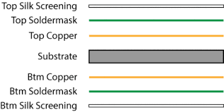
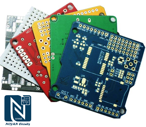
در بردهای مدارچاپی علاوه بر لایه های مس رو، مس زیر و زیرلایه (substrate)، لایه های دیگری نیز بکار می روند که در شکل زیر نشان داده شده اند. بعد از لایه مس روی برد لایه محافظ قلع کاری (Solder Mask) استفاده می شود و پس از آن چاپ راهنما (Silk Screen) اعمال می گردد. برای زیر برد نیز با توجه به نیاز می توان از این لایه ها استفاده نمود.
– چاپ سلدر یا چاپ محافظ قلع کاری (Solder Mask):
چاپ محافظ قلع کاری یک لایه نازک پلیمری لاک مانند است که معمولاً بر روی محلهایی از خطوط مس که محل نصب قطعه و قلعکاری نیستند، مورد استفاده قرار می گیرد. این چاپ علاوه بر زیبایی و محافظت در برابر اکسید شدن فیبر و ترک های مسی در برابر انواع مسائل محیطی، باعث می شود اتصال ناخواسته ای که هنگام لحیم کاری پایه های نزدیک به هم با هویه ایجاد می شود (Solder Bridge) به راحتی از هم جدا شود، همچنین در وان قلع از اتصالات اضافی و تغییر رنگ فیبر در وان که حرارت زیادی دارد جلوگیری می کند. این پوشش در رنگ های مختلفی مانند سبز، سفید، قرمز، آبی و … وجود دارد اما به علت اینکه پوشش سبز رنگ بیشترین استفاده را دارد سولدر ماسک بصورت عامیانه به نام چاپ سبز هم شناخته می شود.
سولدر ماسک به چندین روش روی برد های مدار چاپی اعمال می گردند. که چند نمونه از آن ها، عبارتند از:
- Epoxy Liquid
- Liquid Photoimageable Solder Mask (LPSM or LPI)
- Dry Film Photoimageable Solder Mask (DFSM)
که با توجه به شرایط مقاومتی مدنظر در محیط، می توان یکی از این نوع ها را استفاده نمود. به عبارتی با توجه ابعاد فیزیکی برد، سوراخ ها، المان ها و مسیرها و با توجه به کاربرد برد و هزینه اعمال سولدر ماسک، متناسب ترین روش انتخاب می گردد. ارزان ترین آن ها مایع اپوکسی است که روی برهای مدار چاپی زده می شود.
Epoxy Liquid
Silk-screened onto the PCB pattern, epoxy liquid is the lowest cost type of solder mask. Epoxy is a thermosetting polymer that has many applications. Silk-screening is a printing technique that uses a woven mesh to support ink-blocking stencils or patterns. The mesh creates open areas for ink transfer. Silk is often used in art but synthetic fibers are more common for electronic applications. The final finishing process involves thermal curing.
Liquid Ink Photoimageable
Liquid photoimageable solder mask (LPSM or LPI) is delivered as an ink formulation.If you have complex surface features, then you’re probably better off with a liquid (LPSM) option for better contact with the copper of your traces and the laminate. LPI solder mask is an epoxy based material, so it is very durable and nearly impossible to remove once they have been cured. There is a variety of methods to apply LPISM ink, such as screen printing, curtain coating, electrostatic spray, air spray and so on.
Liquid Photo Imageable Solder Mask is normally applied to printed circuit board in the following steps:
1. The plate should be thoroughly cleaned to ensure no dust particles are trapped on the surface.
2. The plates are completely covered on both sides with the liquid mask.
3. The coated plates are placed in an oven to tack-dry the mask.
4. A film is made of the solder mask Gerber files. Where you want to apply mask to the board, the film will be clear. Where the mask should be removed will be black on the film.
5. The tack-dried boards are placed into a UV developer and the film is precisely aligned over the board. The black area on the film will prevent the UV light from curing the mask where it is not wanted.
6. After the mask is exposed to the UV lamps, the uncured mask is washed off.
The downside to a liquid application is that the thickness isn’t perfectly uniform across the board.
We will introduce detailed applying methods in next articles. Please check silk screen printing, curtain coating, electrostatic spray, air spray.
another type of process commonly used with liquid ink formulations is hot air surface leveling (HASL). It requires a clean environment, free of particles and contaminants. After the UV light exposure stage, the mask is removed using high-pressure water sprays called developers. Circuit board finishing requires thermal curing and organic coating.
Dry Film Photoimageable
Dry Film Photoimageable Solder Mask (DFSM) is applied using vacuum lamination onto the board to avoid creating defects with air bubbles, then exposed and developed. After developing, openings are created in the pattern and parts can be soldered to the copper pads. Copper is layered onto the board inside the holes and on the trace areas using electrochemical processing. Tin is applied to protect the copper circuitry. The dry film is then removed and the exposed copper etched. Finishing also involves thermal curing. A dry application lays down a uniform thickness across the entire surface. However, dry mask adheres best if your board surface is very flat. There are some negative factors using dry film:
On the surface of PCB boards there are pads, lines, so the surface is not smooth, and the dry film solder mask has no liquidity. So, between the dry film and the surface of the circuit board there may be the gas left. The gas gets expanded when heated, which may cause dry film rupture phenomena. Dry film is relatively thick, generally the thickness is 0.08 ~ 0.1mm (3 ~ 4mil). The dry film covering on the surface of circuit boards, may cause the offset phenomenon. Curing conditions of dry film solder mask is very strict, if the curing temperature is too low or the curing time is too short, then the curing is insufficient. It will be affected by the solvent while cleaning. If the curing is too brittle, it may crack when exposed to heat stress. What’s more, dry film solder resist has poor resistance to thermal shock, easy to get cracked in high temperature. The price of dry film is high than wet film.
How thick should my solder mask be?
The thickness of your solder mask primarily depends on how thick the copper traces on your board. In general, you’ll want about 0.5 mils of solder mask over your traces. If you use a liquid mask, you’ll necessarily have a varying thickness over other features. Over empty laminate areas, you can expect a thickness of 0.8-1.2 mils, and over complex features, like the knee of a circuit, it might be as thin as 0.3 mils.
Like any other fabrication parameter or process, you should consider how sensitive your final application will be, and plan your design accordingly. It’s always important to discuss the fabrication options with your manufacturer. They may even be able to suggest better options based on their capabilities.
Standards
Information on the use of solder mask is contained in IPC-SM-840C Qualification and Performance of Permanent Solder Mask. The specification is intended to facilitate evaluation of solder mask by a vendor using a standard board system, and to enable designer, manufacturer, and user together to qualify a production board process.
The test methods and conditions in IPC-SM-840C are based on end use and environmental reliability requirements for two classes1 of user:
1 Older IPC documents refer to Class 1, Class 2, and Class 3. For all practical purposes there is no Class 1 solder mask; Class 2 is equivalent to Class T; Class 3 is the equivalent of Class H.
T – Telecommunication (includes computers, telecommunication equipment, sophisticated business machines, instruments, and certain non-critical military applications.) Solder mask on boards in this class is suitable for high performance commercial and industrial products in which extended performance life is required, but for which interrupted service is not life-threatening.
H – High Reliability/Military (includes that equipment where continued performance is critical, equipment down-time cannot be tolerated and/or the equipment is a life support item). Solder mask on boards of this class is suitable for applications where high levels of assurance are required and uninterrupted service is essential.
IPC-SM-840C divides responsibilities between materials supplier, board fabricator and board user. The user’s task is to “monitor the acceptability and functionality of the completed boards”. Note particularly that IPC-SM-840C specifically does not “determine the compatibility of solder mask materials with post-soldering products and processes” – if you want to conformal coat the final product, it becomes your responsibility to check for compatibility.
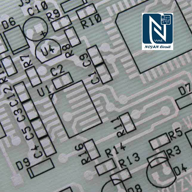
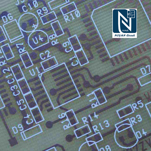
– چاپ راهنما یا مارکاژ (Silk Screen):
چاپ راهنما تحت عنوان چاپ مارکاژ و سیلک اسکرین شناخته می شود که محل قرار گیری قطعات الکترونیک، نقاط تست، شماره المان، لوگوی شرکت و علائم هشدار را روی فیبر مدار چاپی مشخص می کند. این چاپ معمولاً در رنگ های سفید و مشکی وجود دارد ولی رنگ های غیر معمولی مثل زرد هم وجود دارد که طبیعتاً روی هزینه و زمان آماده سازی تاثیر خواهد گذاشت. مطابق با استاندارد های IPC باید نشان تولید کننده و شماره رهگیری محصول حتما روی برد قید شود تا امکان پیگیری مشکلات احتمالی در آینده وجود داشته باشد اما جای مشخصی برای آن ها روی برد مدارچاپی در این استاندارد تعیین نشده است. معمولا این دو نشان در جایی که نسبت به بقیه قسمت های برد تراکم کمتری دارد و جای حساسی نیست، گذاشته می شوند.